Lesson 3
Computing
Foundations - Learning Outcome 1:
Identify and describe the major types of computer systems.
Identify and describe the major performance issues.
1.1 Identify and describe the various types of PC hardware systems (mainframe, mini and microcomputer).
1.2 Compare and contrast the major types of computer hardware systems.
1.3 Define and describe the basic units of memory measurement including bit, byte, kilobyte, megabyte and gigabyte.
1.4 Compare various hardware items in terms of memory capacity, CPU clock speed, disk storage space and I/O services available.
Handout: Glossary of terms.
Theory:
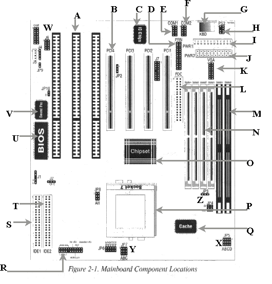
Motherboard Component Identification
1. Component A represents what type of bus slots?
_____________________________________________________________________
2. Component B represents another type of bus slot. What is the name of this bus slot?
_____________________________________________________________________
3. Name three other bus slot types?
_____________________________________________________________________
4.
Name all the bus types considered to be local buses.
_____________________________________________________________________
5. The AGP bus slot is not present on the motherboard shown in fig. 2-1. What type of adapter card is likely to be found in an AGP bus slot, and why?
_____________________________________________________________________
_____________________________________________________________________
6. The “Integrated Circuit” that C refers to is labeled “IO Chips”. What do you think may be the role of this chip?
_____________________________________________________________________
7. What is the component that D refers to and what I/O address is it generally allocated?
_____________________________________________________________________
8. There are a number of modes that can be set for D by the user in the BIOS setup program. Name all these modes and explain when you would use them.
_____________________________________________________________________
_____________________________________________________________________
_____________________________________________________________________
_____________________________________________________________________
_____________________________________________________________________
9. Component E & F are labeled COM1 and COM2 respectively. What type of components are these and what I/O addresses and IRQ numbers can be allocated to these components?
_____________________________________________________________________
_____________________________________________________________________
_____________________________________________________________________
10. A common mistake with modem installation involves the settings for the serial port. What speed and “flow control” type should be set for a serial port attached to a modem?
_____________________________________________________________________
11. Two types of connectors can be attached to COM1 & COM2. Name these two socket types and state a device that is commonly attached to each of them.
_____________________________________________________________________
12. Component G refers to the keyboard socket. There are two other common types of keyboard sockets. What are their names? What file would you change and what changes would you make to ensure success?
_____________________________________________________________________
13. Component H is labeled “PS2”. A PS2 socket is often attached to this port. What serial device is often connected to this socket?
_____________________________________________________________________
14. What IRQ number is generally allocated to the PS2 port and where can this port be disabled if necessary?
_____________________________________________________________________
15. J & I represent two types of common motherboard power supply connectors. What names are given to them and which one is the latest type?
_____________________________________________________________________
16. The motherboard shown in fig. 2-1 has both sound and video onboard. What type of output connector is attached to component K and what peripheral device is subsequently connected?
_____________________________________________________________________
17. Four video modes for monitors are CGA, EGA, VGA and SVGA. Name the monitor types that are (pin-for-pin) compatible?
_____________________________________________________________________
18. The interface that L refers to is labelled “FDC”. What does “FDC” stand for and what types of peripheral devices are connected to this interface?
_____________________________________________________________________
19. Where must the peripheral device in question 18 first be enabled and what are the capacity options generally offered?
_____________________________________________________________________
20. A ribbon cable provides a connection between the FDC and the attached peripheral devices. How many of these peripheral devices can be attached to the FDC and what is the purpose of the twisted portion of the cable near the end?
_____________________________________________________________________
21. M refers to two long dark slots. What important component(s) do these slots house and why do these components have so many pins?
_____________________________________________________________________
22. The components in question 21 come in a variety of sizes and access times. What access times are required for motherboard with 100 MHz bus speeds?
_____________________________________________________________________
23. The data bus on the motherboard in fig. 2-1 has 32-bit access to the CPU. What size is the data bus to the components in question 21?
_____________________________________________________________________
24. Z refers to jumpers that select the voltage required for the component in question 21. What are the two voltage options and what voltage is generally selected?
_____________________________________________________________________
25. N refers to sockets that house similar components to those of question 21. What components may be inserted in these sockets and how do they differ from the types used in question 21?
_____________________________________________________________________
26. What is the minimum number of components that can be inserted into the sockets of question 25 for normal operation of the PC?
_____________________________________________________________________
27. O refers to a motherboard component labelled “Chipset”. Explain the major functions of this component.
_____________________________________________________________________
_____________________________________________________________________
_____________________________________________________________________
28. What important component is inserted into the socket referred to by P?
_____________________________________________________________________
29. Could a Pentium II or III be inserted into this socket? Give reasons for your answer.
_____________________________________________________________________
30. JP5, JP6, JP7 and JP8 are jumper switches for setting CPU internal and external bus speeds (see areas denoted by X and Y). They also set the CPU voltage levels. Where can the accuracy of the CPU jumper settings be viewed for confirmation and what signs of too high bus speeds would you look for?
_____________________________________________________________________
_____________________________________________________________________
31. State the name, purpose and typical values associated with the component referred to by Q? Also state why this component is considered very fast.
_____________________________________________________________________
_____________________________________________________________________
32. There is another type of cache available onboard the CPU. What is its name and why does this cache type make the “Celeron” processor so fast?
_____________________________________________________________________
33. The pin array that R refers to provides many functions. Name at least four.
_____________________________________________________________________
34. The two IDE interfaces that T & U point to, support two devices each. Name two common devices that are attached to an IDE interface.
_____________________________________________________________________
35. The motherboard diagram does not show pin 1 designation for the IDE interfaces. Why would the location of pin 1 be important?
_____________________________________________________________________
36. IDE type (Ultra ATA 66, Ultra DMA, EIDE, IDE) hard drives can be connected to IDE interface ports. They must be configured as a master or slave drive using a jumper provided locally. If two hard drives are mounted on the one IDE port, what would be the jumper setting for the bootable hard drive using the Windows 95 operating system?
_____________________________________________________________________
37. The component that U refers to is considered firmware. Explain the important role of the BIOS, what BIOS stands for, and why it is considered firmware.
_____________________________________________________________________
_____________________________________________________________________
38. Somewhere on the motherboard (not shown) is a chip referred to as CMOS (often has the part number “4069”). What is the purpose of the CMOS chip and where does it get the power to keep settings when mains power is disconnected?
_____________________________________________________________________
_____________________________________________________________________
39. V points to another chip, labelled Sound Pro. The interface ports for external connectors to be attached for sound can be found around the vicinity of W. Name two methods used to disable onboard devices such as sound and video.
_____________________________________________________________________
40. What important software should you receive with this motherboard?
_____________________________________________________________________
41. The importance of documentation relating to your motherboard cannot be overstated! If you were a network administrator with 100 or more PC’s in your charge, with many different types of motherboards installed, how would you organise your documentation (you will required to seriously consider this in the future).
_____________________________________________________________________
_____________________________________________________________________
_____________________________________________________________________
_____________________________________________________________________
42. How many bytes is a kilobyte?
_____________________________________________________________________
43. Why is a hard drive labelled as having a 13 Gigabyte capacity, detected as being approximately 12 Gigabytes?
_____________________________________________________________________
_____________________________________________________________________
Practical: Motherboard Component Identification
Aim: To introduce students to multiple types of PC motherboard configurations and draw their attention to many components shared by most motherboards.
Resources: Wide range of motherboards (286 to Pentium): Preferably, one per student.
Procedure:
You are required to sketch the motherboard you are given by the teacher. The sketch must clearly label all components mentioned in theory lesson 3.
Typically,
you would include the following motherboard components:
FDC interface
IDE interface
RAM slots and type
Chipset
Power connectors and type
Serial Ports
Parallel Port
Keyboard Socket and type
Buses and types
BIOS chip
CPU socket and type
Maths Co-Processor socket (if present)
External cache chips
Additional non-standard components
Compiled by: Wayne Shirley 7/99